 EN
EN  CN
CN
Why Do Semiconductor Manufacturers Prefer 99%+ High-Purity Alumina Ceramics?
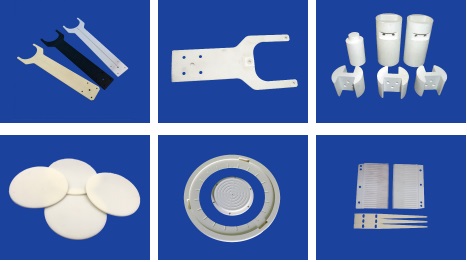
In the processes of semiconductor manufacturing, alumina ceramics have become an indispensable key material due to their excellent electrical insulation, high hardness, resistance to plasma erosion, and good thermal conductivity. They are primarily used for high-purity ceramic structural components in wafer handling and etch chambers.
These critical semiconductor ceramic components include:
Vacuum and electrostatic chucks used to secure wafers and withstand high temperatures and corrosive gases;
Liners and focusing rings that protect the inner walls of plasma etching chambers and reduce particle contamination;
Process chucks that prevent metal contamination and support wafers;
Precision air-bearing guide rail bases that provide ultra-stable support in lithography and inspection equipment.
High purity alumina ceramic tube for semiconductor equipment.
......
The purity requirements for these components are at least 99% alumina or even 99.5% or higher, far exceeding the 92%–96% Al₂O₃ used in typical industrial applications. The reasons behind this can be understood from the following perspective. Why 99%+ purity alumina ceramics are essential for semiconductor applications?
1. The plasma environment continuously erodes the ceramic surface
The etching process uses halogen plasmas (Cl₂, HBr, fluorinated gases), which are extremely high in energy and subject the inner walls of the chamber to a dual attack of continuous chemical corrosion and physical sputtering. In terms of chemical corrosion, halogens react with oxides in the ceramic, forming volatile byproducts on the alumina surface that erode it layer by layer. In terms of physical sputtering, high-energy ions directly bombard the surface, ejecting material atoms one by one. As a result of these combined effects, material from the chamber surface is continuously released into the chamber environment in the form of particles or atoms. If impurities are present within the chamber, they will become sources of contamination on the wafer.
2. The Damage Caused by Metal Impurities to Chips Is Catastrophic
Impurities remaining in alumina are primarily divided into two categories, each with distinctly different failure mechanisms:
- The first category consists of alkali metal ions, represented by Na⁺ and K⁺. These ions exhibit extremely strong mobility within silicon devices. Once they enter the gate oxide layer, they cause the threshold voltage of MOS devices to drift, rendering the transistor’s switching characteristics unstable. Furthermore, this failure is progressive; as temperature fluctuations and electric fields drive migration during operation, the ions continue to migrate, causing device characteristics to deteriorate continuously.
- The second category consists of transition metals, such as Fe, Ni, and Cu. These elements form deep-level defects in silicon, acting as recombination centers for minority carriers, which significantly shortens minority carrier lifetime. This directly manifests as increased diode leakage current, reduced device response speed, and degraded p-n junction characteristics.
This explains why 96% alumina, which performs well in industrial applications, is inadequate for semiconductor cavities. Although the difference between 96% and 99.8% alumina is only 3.8%, the total impurity content can differ by more than one order of magnitude.
3. High-Temperature Vacuum Environment Demands Greater Thermal Stability
Semiconductor processes frequently involve high-temperature diffusion furnaces, oxidation furnaces, PECVD/etching equipment, and vacuum heat treatment systems. Since wafers are highly susceptible to contamination from particulates, these processes are typically conducted in vacuum environments. Under these demanding conditions, materials used for ceramic robotic arms must maintain excellent thermal stability, low particle generation, and mechanical reliability. Therefore, ceramic materials must provide excellent high-temperature stability, wear resistance, low outgassing, and high mechanical strength. Due to these demanding operating conditions, high-purity alumina ceramics are widely preferred.
4. Superior Mechanical Properties and Dimensional Stability
High-purity alumina typically features lower porosity and higher density, resulting in greater strength, reduced deformation, better dimensional stability, and tighter achievable tolerances after machining. These properties make high-purity alumina ceramics suitable for a wide range of semiconductor applications:
- Low impurity levels
- Electrical insulation
- Plasma resistance
- Dimensional stability
High-temperature stability
High-purity alumina ceramic components are critical parts in semiconductor manufacturing equipment. Driven by the growth of artificial intelligence, cloud computing, and data center infrastructure, semiconductor demand continues to increase, creating new opportunities for high-performance alumina ceramic components.